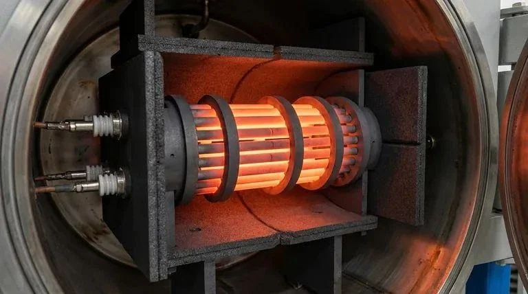
A thermal pad does not cool a device by itself. Heat still needs a complete route from the silicon junction to a larger surface, a frame or an active cooling element. A thin graphite layer earns its place when a concentrated hot spot must spread across more area before the next interface. That is the path followed here: chip, first interface, graphite spreader, chassis contact and final rejection to the surrounding air or coolant.
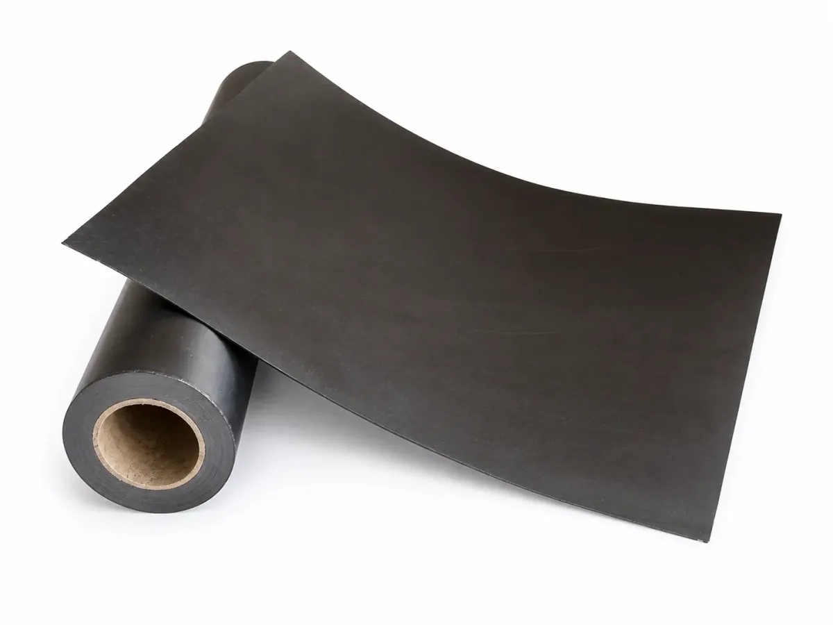
QDZRT Graphite supplies expanded-natural-graphite paper and foil in thin sheet and roll forms, subject to the named grade, thickness, density and project requirements. These materials are produced from natural graphite through expansion and calendering, then may be slit, laminated, die-cut, insulated or backed with adhesive by the agreed conversion route. They must not be presented as the same product family as synthetic or pyrolytic graphite sheet. Both can spread heat, but their manufacturing route, thickness range, directional properties, mechanical behaviour and available laminate constructions differ. The design question is therefore not merely “Does graphite conduct heat?” It is “Which graphite construction is being specified, where does heat enter, how far must it travel sideways and where can it leave?”
Where the Heat Starts
The hot spot is the starting point, not the specification. Heat begins at a small active region inside a component, while the package, shield or enclosure may cover a much larger area. A processor, power transistor, LED array, radio-frequency device or battery connection can therefore create the same design mismatch: a compact source releases heat faster than the nearby structure can accept it. The local junction or case temperature rises first; the outer enclosure responds later. The required spreader cannot be selected from device category alone because the active footprint, duty cycle, package construction and receiving surface determine the actual heat path.
The path contains several thermal resistances in series. Heat crosses the die attach, package lid or mould compound, a gap material, the graphite pad, another adhesive or insulation layer and finally the chassis. A low resistance in one layer cannot cancel a poor contact elsewhere. A 25 µm graphite sheet with strong in-plane conduction will still disappoint when a 150 µm air gap sits under half of its area. Air is the weak link, not the carbon.
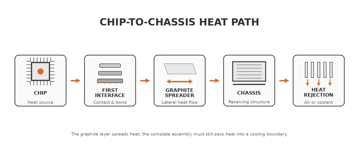
Start with power and area. Ten watts spread from a 10 mm × 10 mm source creates 0.10 W/mm² at that idealized footprint. The same 10 W distributed across a 60 mm × 80 mm receiving area corresponds to about 0.0021 W/mm². This arithmetic does not predict device temperature, contact resistance or lateral spreading efficiency; it only shows why enlarging the area presented to the next structure can reduce concentration. Thin anisotropic materials are considered in compact electronics for this reason, but every number must remain attached to a defined source, geometry, material direction and boundary condition.
| Illustrative case | Power input | Source footprint | Initial heat flux | Idealized receiving area | Flux after ideal area redistribution |
|---|---|---|---|---|---|
| Case A | 8 W | 12 × 12 mm = 144 mm² | 0.0556 W/mm² | 55 × 75 mm = 4125 mm² | 0.00194 W/mm² |
| Case B | 18 W | 15 × 20 mm = 300 mm² | 0.0600 W/mm² | 70 × 90 mm = 6300 mm² | 0.00286 W/mm² |
| Case C | 25 W | 20 × 30 mm = 600 mm² | 0.0417 W/mm² | 100 × 120 mm = 12000 mm² | 0.00208 W/mm² |
| Case D | 12 W | 18 × 18 mm = 324 mm² | 0.0370 W/mm² | 60 × 60 mm = 3600 mm² | 0.00333 W/mm² |
| Case E | 45 W | 30 × 40 mm = 1200 mm² | 0.0375 W/mm² | 120 × 150 mm = 18000 mm² | 0.00250 W/mm² |
These five cases are arithmetic examples, not typical ratings for named devices and not guaranteed temperature reductions. A real result depends on package construction, source distribution, contact pressure, orientation, adhesive or insulation layers, the size and temperature of the receiving surface and the final cooling boundary. Our overview of graphite in thermal management places sheet materials beside blocks and machined components, while the thermal-management solution page shows why product form must follow the actual location and direction of heat flow.
The First Interface: Chip to Spreader
Contact failure can erase a good material choice. The first interface turns a drawing into a thermal contact, and a chip lid or shield can look flat while still containing bow, texture and height variation. Pressure closes part of the microscopic gap; a compliant adhesive or interface layer fills another part. Any remaining void becomes a thermal barrier. The pad therefore needs enough real contact area to collect heat without creating excessive mechanical load on the component, and its test condition should state pressure, surface preparation, temperature and specimen construction.
Adhesive simplifies assembly but adds resistance. A 25 µm pressure-sensitive adhesive on each face can equal or exceed the thickness of a 25 µm graphite core. The adhesive also changes shear behaviour during thermal cycling. A very soft layer accommodates movement but allows the graphite to drift. A stiff layer controls position but transfers more strain into the edge of the sheet. Release liner, adhesive coat weight and lamination direction belong in the production specification.
Electrical isolation is a separate requirement. Graphite conducts electricity. A pad that can touch exposed contacts, antenna structures or battery terminals needs an insulating film or a geometry that maintains creepage distance. That film adds another interface and can restrict heat flow through the thickness. The assembly stack must state whether the pad is electrically floating, grounded to the chassis or fully insulated.
A converter can compare raw material, adhesive and protective-film routes with the discussion of graphite paper pad conversion. The distinction between flexible expanded-natural-graphite foil and engineered synthetic thermal sheet also matters; the foil-versus-thermal-sheet comparison explains why a trade name alone does not define directional conductivity or layer construction. For through-thickness test planning, ASTM D5470-17(2024) measures thermal impedance under specified steady-state conditions and warns that those idealized results cannot be applied directly to every practical assembly.
| Illustrative layer | Example thickness | Conductivity used only for arithmetic | Common reference area | Calculated ideal layer resistance | Assembly concern |
|---|---|---|---|---|---|
| Package interface film | 20 µm | 0.30 W/m·K | 900 mm² | 0.074 K/W | Coverage, pressure and voids |
| Pressure-sensitive adhesive 1 | 25 µm | 0.20 W/m·K | 900 mm² | 0.139 K/W | Coat uniformity and contact |
| Graphite core | 40 µm | 5 W/m·K through-plane | 900 mm² | 0.0089 K/W | Direction and named grade |
| Pressure-sensitive adhesive 2 | 25 µm | 0.20 W/m·K | 900 mm² | 0.139 K/W | Bond to receiving surface |
| PET insulation film | 12 µm | 0.15 W/m·K | 900 mm² | 0.0889 K/W | Electrical isolation and coverage |
| Air void | 100 µm | 0.026 W/m·K | 900 mm² | 4.27 K/W | Can dominate the local path |
The table uses the ideal one-dimensional relation R = thickness ÷ conductivity ÷ area and applies one common 900 mm² reference area so that the arithmetic is comparable. It is not a product certificate, a full assembly model or an ASTM D5470 report. Contact resistance, pressure, surface condition, temperature, alternate heat paths and material heterogeneity can change the measured result. The air-void row is included to show scale: even at the same reference area, a thin void can contribute far more ideal resistance than the solid layers.
Spreading Sideways: Why In-Plane Matters
Sideways conduction is the core job, but the material family and manufacturing route must be identified. Expanded-natural-graphite foil is made by expanding and calendering natural graphite; SGL Carbon’s SIGRATHERM foil description is one supplier example of that route. Synthetic pyrolytic graphite sheet is manufactured differently and is sold in specific grades and constructions; Panasonic’s EYGS091207 page, for example, identifies a named 70 µm PGS-only product with its own conductivity value. Data from either family must remain attached to the exact named product, test direction and construction.
Distance consumes spreading capacity. Heat injected at the centre can move in every in-plane direction. Heat injected near a cutout, screw boss or sheet edge has fewer paths and creates a higher gradient. A long narrow strip transfers heat well along its length only when fibre or sheet orientation, adhesive pattern and contact area remain continuous. Slots that simplify folding may interrupt the path.
Thermal conductivity values need a direction, method and condition. A single number without “in-plane” or “through-plane” is incomplete, and the same applies to diffusivity, density, thickness and laminate state. A NASA study on pyrolytic graphite sheet integration evaluates PGS embedded in a carbon-fibre polymer radiator concept. It supports the principle that a highly directional synthetic sheet can be integrated into a specific lightweight composite thermal structure; it does not validate every commercial graphite paper, bare PGS grade, adhesive laminate or chip-to-chassis assembly.
The spreader usually needs usable area beyond the hot source, but no fixed extension distance is universal. The drawing and validation plan needs to define the source footprint, candidate receiving zones, available routing around connectors and keep-outs, sheet orientation, edge distance, adhesive coverage and the maximum permitted outline. Simulation or an instrumented prototype can then compare candidate extensions and reveal whether the added area actually reaches a cooler structure. A longer pad that ends on a thermally isolated plastic region may add cost and handling risk without improving heat rejection.
For applications that require a broad product description before conversion details, the article on graphite paper properties and selection and the thickness and density selection guide separate sheet dimensions from functional requirements.
Getting Heat to the Chassis
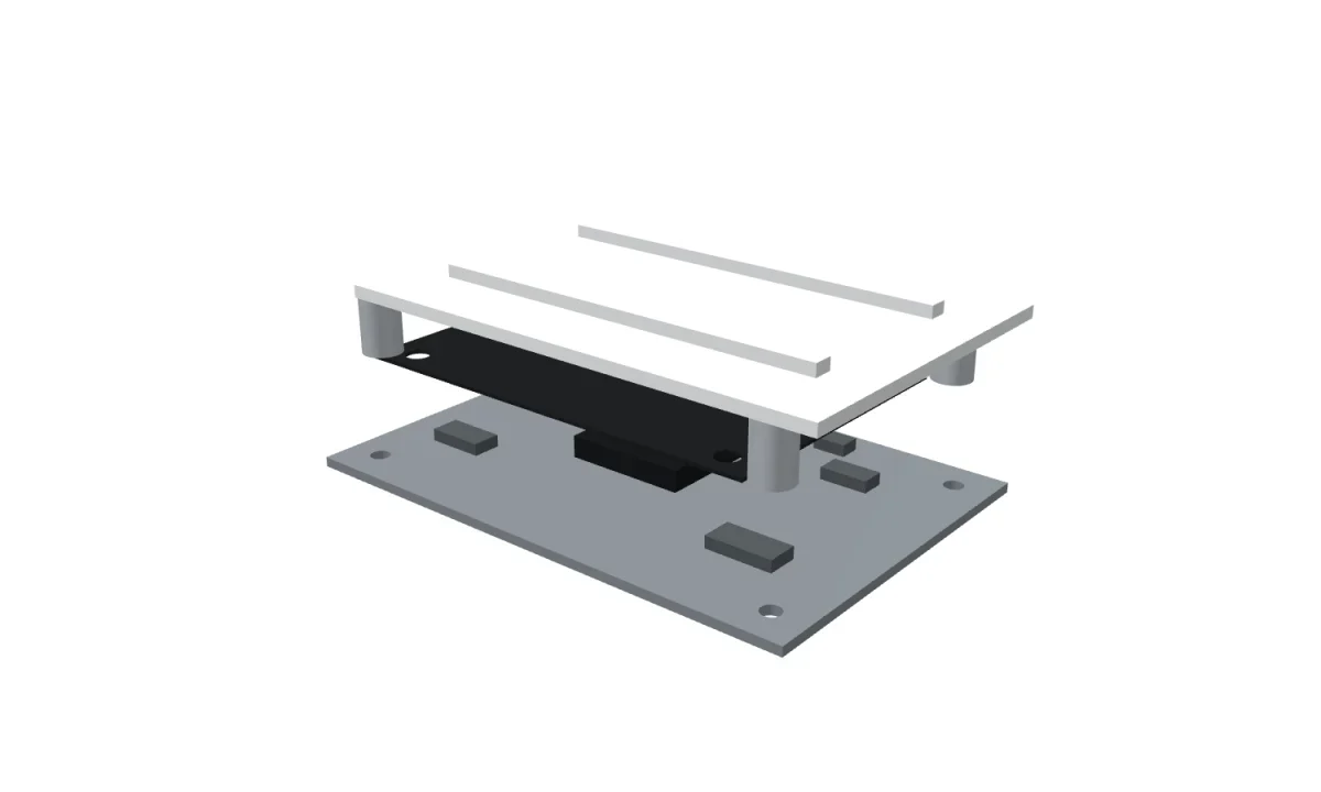
A spreader still needs somewhere to discharge heat. Spreading sideways is only the middle of the journey; heat must cross into the chassis, frame, battery cold plate or secondary heat sink. A graphite pad bonded over a larger area can lower a local peak while the average receiving-structure temperature rises. That response can be expected because the frame is accepting more energy. The final design still needs enough area, airflow, conduction to another structure or liquid cooling to reject the same input power.
Contact at the receiving end can be full-area, edge-bonded or compressed under a bracket. Full-area bonding offers the largest contact but makes rework difficult. Edge bonding preserves a cleaner central thermal route yet can leave bubbles. Mechanical compression permits disassembly, although pressure must remain uniform and cannot crush nearby components. Each method changes the drawing and inspection plan.
A metal chassis spreads heat in three dimensions; graphite accelerates the first lateral movement. Copper and aluminium are not competitors that must be removed. They often form the receiving structure. A hybrid stack can use graphite to move heat away from the chip, aluminium to store and distribute energy through the enclosure and convection to release it. The choice depends on mass, thickness, electrical constraints and cost.
Instrument the entire path during validation. Place one thermocouple near the heat source, several along the graphite extension and at least one on the far chassis zone. Record steady state after temperatures stop changing, then repeat during a power pulse. Infrared imaging can show lateral patterns, but emissivity differences between graphite, adhesive and metal can distort absolute readings unless the surfaces are prepared consistently.
Once the heat path is validated, the packaging and logistics guidance becomes relevant because thin converted pads must reach the assembly plant without creasing, edge damage, contamination or liner displacement. Packaging requirements should preserve the tested orientation, flatness and stack construction rather than treating the part as an unprotected piece of sheet material.
Thickness Budget in a Thin Device
Installed thickness is the number the device sees. A thin device rarely has spare height, so the drawing needs a complete stack-up rather than a nominal sheet thickness. Graphite core, adhesive coats, liner removal, optional insulation, local overlaps and compression state all affect the final assembly. A “0.10 mm pad” could mean a 0.10 mm graphite core or a 0.10 mm total laminate; those are different products with different contact, electrical and handling behaviour.
Tolerance can consume the gap. Suppose the available space is 0.20 mm with ±0.05 mm mechanical variation. A 0.12 mm laminate at ±0.02 mm leaves only 0.01–0.15 mm theoretical clearance before package bow and adhesive squeeze are included. The pad may fail to contact in one unit and create excessive force in another. A thermal spreader cannot compensate for an uncontrolled mechanical stack.
| Stack element | Nominal thickness | Illustrative tolerance | Minimum | Maximum | Status after assembly |
|---|---|---|---|---|---|
| Graphite core | 40 µm | ±5 µm | 35 µm | 45 µm | Remains |
| Top adhesive | 25 µm | ±4 µm | 21 µm | 29 µm | Remains |
| Bottom adhesive | 25 µm | ±4 µm | 21 µm | 29 µm | Remains |
| PET insulation | 12 µm | ±2 µm | 10 µm | 14 µm | Remains if specified |
| Release liner A | 75 µm | ±8 µm | 67 µm | 83 µm | Removed |
| Release liner B | 50 µm | ±6 µm | 44 µm | 56 µm | Removed |
| Installed laminate without liners | 102 µm | RSS arithmetic ±7.8 µm, rounded to ±8 µm | 94 µm | 110 µm | Drawing and process control |
The installed-laminate row uses root-sum-square arithmetic only: √(5² + 4² + 4² + 2²) = 7.81 µm, rounded to 8 µm. That calculation assumes independent, centred contributors and does not prove process capability or guarantee the listed minimum and maximum. If suppliers state limit tolerances, correlated variation, compression behaviour or additional coating uncertainty, the drawing and tolerance analysis must use the approved method instead. Liner values still matter to die-cutting and automatic placement even though the liners disappear from the device; state both shipping thickness and installed thickness on the converter drawing.
Roll width and cut geometry also affect usable material. The roll-quality inspection article covers thickness maps, edges and unwind behaviour, while export packing for rolls and sheets addresses the physical protection needed before conversion.
What Breaks: Delamination, Tear, Contamination
Edges often fail before the bulk material. Converted graphite pads can develop corner lift, tears across narrow bridges, adhesive delamination or conductive fragments in a prohibited area. Folding a laminate around a sharp edge concentrates strain in the graphite layer, while repeated enclosure movement can extend an initial notch. The risk depends on the named graphite construction, laminate direction, corner geometry, liner release, pick-and-place motion and the mechanical support provided during assembly.
Delamination begins at a weak interface. Causes include contamination on the metal, insufficient lamination pressure, adhesive that has aged beyond its storage window and a surface treatment that does not match the adhesive chemistry. The failure can stay invisible until a thermal cycle creates shear between materials with different expansion rates. Peel tests on the actual substrate are more relevant than a generic adhesive data sheet.
Tear risk follows geometry and handling, but no bridge width or positional tolerance is universally safe. Internal corners need an approved radius, narrow necks need enough width for the selected material and conversion method, and pull tabs must transfer peel force through the liner rather than through an unsupported graphite core. A design review should record the minimum web, corner radius, peel direction, tool condition, liner release, placement method and acceptance test. Prototype handling data may justify widening a bridge or changing peel direction, but those dimensions remain project-specific.
Contamination control is both thermal and electrical. Dust between adhesive and chassis creates local voids, while loose conductive fragments can migrate toward contacts. Gloves, clean liners, covered trays and suitable extraction reduce transfer, but the control method must match the actual cutting or slitting task. For U.S. occupational-health context, NIOSH lists natural graphite separately from synthetic graphite. The material identity, local law, SDS, task, exposure assessment and measured control performance must be established before an exposure limit is used; the natural-graphite entry should not be copied automatically into a synthetic-graphite process, or vice versa.
Related production risks appear in our production and delivery management article and global project communication guidance, where revision identity and packaging information remain connected to the material supplied.
Specifying the Pad for Production
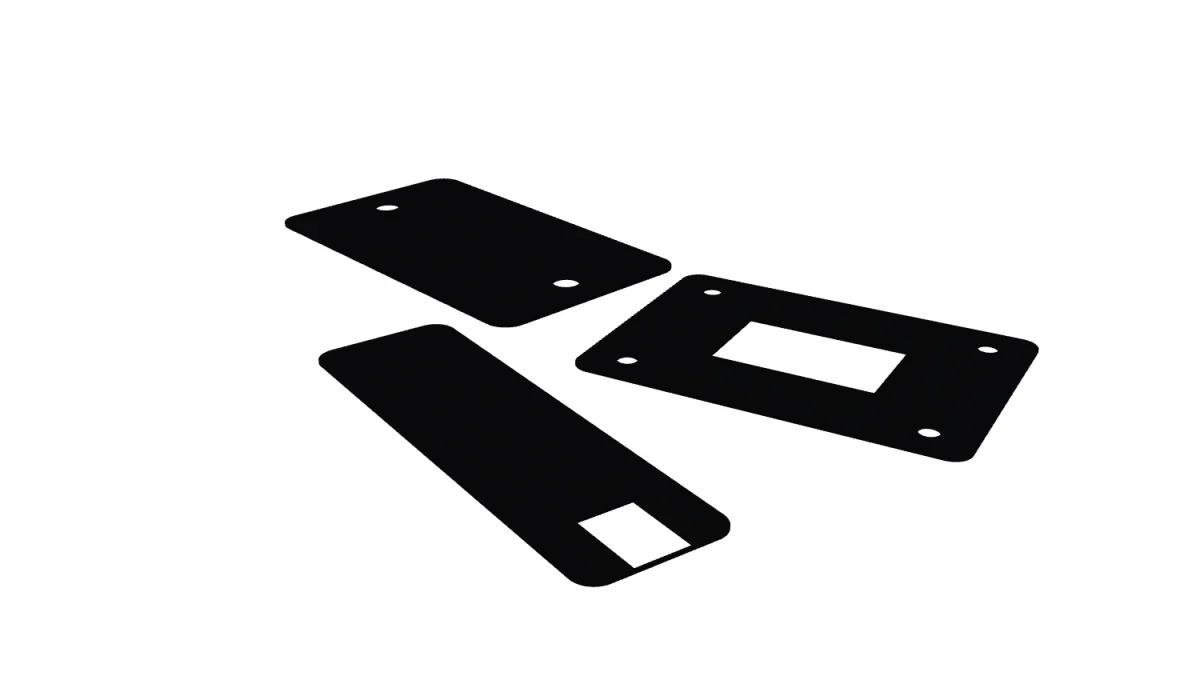
A production specification starts with the heat path. Identify the source footprint and power, the receiving chassis area, the maximum installed thickness and every electrical keep-out. Then define the material construction: graphite core thickness and density, in-plane thermal requirement where available, adhesive on one or two faces, insulation film, liner type and finished outline revision.
The drawing must distinguish cut-through from kiss-cut features and identify orientation, part pitch, roll direction, tabs, holes, corner radii, registration features and the controlling file revision. Positional and outline tolerances should follow assembly function and demonstrated conversion capability rather than a generic value. Tight controls belong where they protect connector clearance, source contact, registration or automated placement; non-functional edges can often use a different visual or dimensional acceptance rule.
Before release, build one validation matrix that connects drawing revision, pad construction and thermal result. Test an unmodified control assembly, the proposed graphite construction and the relevant boundary conditions, such as maximum input power, minimum contact pressure, high ambient temperature or the least favourable receiving-surface condition. Record source temperature, receiving-structure temperature, ambient condition, input power, sensor location, sampling interval and the definition of steady state. Repeat enough units to reveal assembly variation, then inspect selected units for edge lift, tears, adhesive transfer, insulation damage and graphite migration. The program owner should approve the allowable temperature change, electrical keep-out, delamination length, particle limit and any rework rule. These values belong in the validated device record; they are not default limits published by our team or universal graphite-paper specifications.
Inspection follows the functional risk. Measure overall laminate thickness at a defined number of points, confirm outline with a fixture or optical system and inspect exposed adhesive, burr-like graphite protrusions, wrinkles and trapped particles. A short thermal test can compare source and chassis temperatures against the approved sample. Record the sample construction so the next roll does not repeat only the product name.
A useful purchase-order line identifies the named graphite construction or approved property envelope, core thickness and density, adhesive system and side, insulation film, installed-thickness requirement, drawing number and revision, roll or part orientation, packaging quantity, electrical keep-out rule and required inspection record. The buyer, converter and material supplier should fill those fields from the approved assembly rather than copying a complete-looking example into a new project.
Our team can discuss expanded-natural-graphite roll or sheet supply and, where the order scope is confirmed, the required lamination direction, slit width, die-cut geometry, insulation or adhesive construction. Final thermal performance, electrical clearance, conversion tolerance, packaging method and validation responsibility must be agreed against the drawing, named material and approved test plan. The graphite paper product page describes the base material form, the graphite products category provides adjacent forms, and the contact page can be used to start the inquiry. After we reply, send the current drawing, stack-up, and other project files by email or another agreed secure channel.
Send the source footprint, power estimate or measured duty, receiving surface, installed-thickness limit, electrical keep-outs, required material family and manufacturing route, laminate construction and validation method together. A defensible selection then follows the complete heat path and named construction instead of treating “graphite paper” as one interchangeable sheet with one conductivity number.
Source-use note: ASTM D5470 is cited for controlled thermal-impedance testing, SGL Carbon for an expanded-natural-graphite foil route, Panasonic for one named synthetic PGS product, NASA for a specific PGS-reinforced composite radiator study, and NIOSH for separate U.S. natural- and synthetic-graphite occupational entries. None of these sources establishes a universal graphite-pad design, a verified process capability for QDZRT Graphite or a guaranteed device-temperature result.